题目
FA25 ECE 555 001 Final
多项填空题
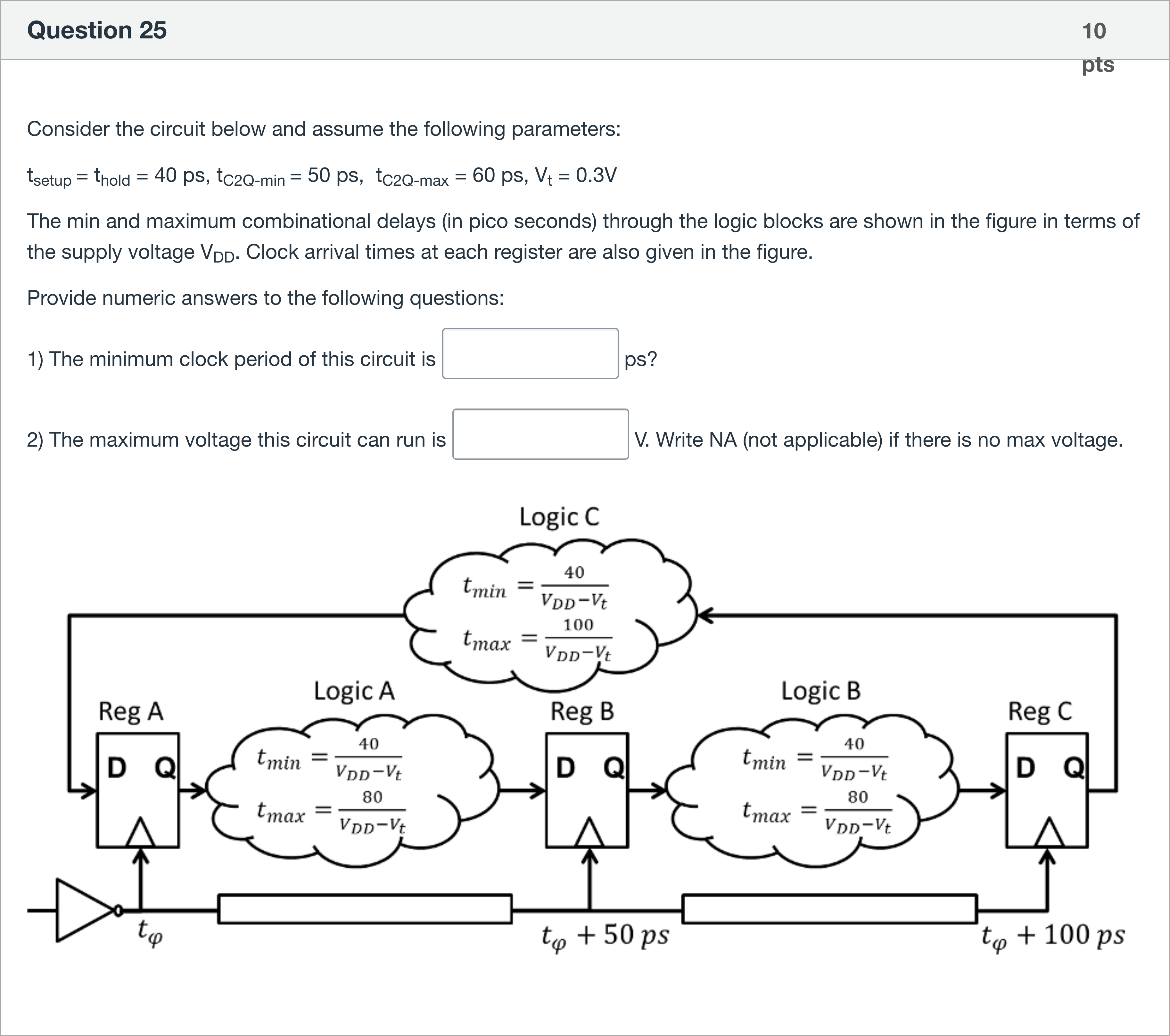
Consider the circuit below and assume the following parameters: tsetup = thold = 40 ps, tC2Q-min = 50 ps, tC2Q-max = 60 ps, Vt = 0.3V The min and maximum combinational delays (in pico seconds) through the logic blocks are shown in the figure in terms of the supply voltage VDD. Clock arrival times at each register are also given in the figure. Provide numeric answers to the following questions: 1) The minimum clock period of this circuit is [Fill in the blank] ps? 2) The maximum voltage this circuit can run is [Fill in the blank] V. Write NA (not applicable) if there is no max voltage.
查看解析
标准答案
Please login to view
思路分析
We begin by restating the problem setup and the data given, then proceed to analyze how the two requested quantities are determined from the timing constraints of the circuit.
- Known parameters: t_setup = t_hold = 40 ps, tC2Q-min = 50 ps, tC2Q-max = 60 ps, Vt = 0.3 V. The diagram indicates that the minimum combinational delay through each logic block is t_min = 40 / (VDD − Vt) and the maximum combinational delay through each logic block is t_max = 80 / (VDD − Vt) (note the factor 80 for the max case as shown in the figure). The clock arrival times at registers are provided in the schematic as well, which affects how the clock period and the maximum operating voltage are computed.
Option analysis for Question 1: The minimum clock period of this circuit is ______ ps
- Step 1: Recall the standard setup/hold timing relation for a synchronous circuit with registers in a single-clock domain. The minimum clock period is governed by the fast (minimum) path from one register’s Q output, through the combinational logic, to the next register’s D input, plus the......Login to view full explanation登录即可查看完整答案
我们收录了全球超50000道考试原题与详细解析,现在登录,立即获得答案。
类似问题
Assume the required time at output f is 5.80. Please calculate the required time for x and the origin. Note: The value inside the circle represents the delay of the gate. The value around the edge represents the delay of the wire. Required time for x: [Fill in the blank], Required time for origin: [Fill in the blank],
Consider the following setup timing report. Fill in the boxes 1 and 2 with the right numerical values (keep 3 decimal places). 1 [Fill in the blank], 2 [Fill in the blank],
In a consumer society, many adults channel creativity into buying things
Economic stress and unpredictable times have resulted in a booming industry for self-help products
更多留学生实用工具
希望你的学习变得更简单
加入我们,立即解锁 海量真题 与 独家解析,让复习快人一步!