Questions
EESM5200 (L2) Quiz 02
Multiple fill-in-the-blank
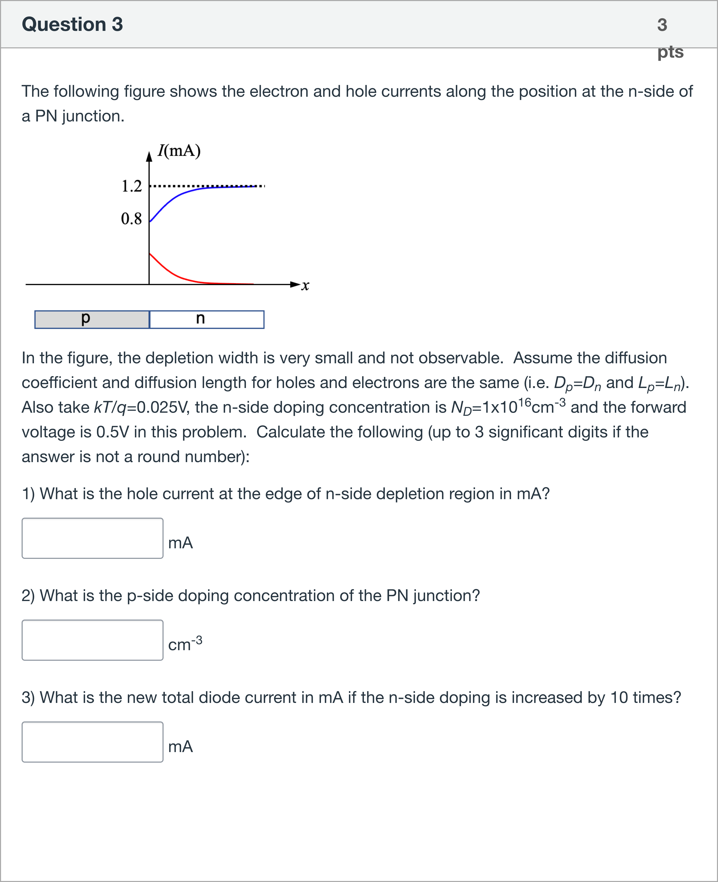
The following figure shows the electron and hole currents along the position at the n-side of a PN junction. In the figure, the depletion width is very small and not observable. Assume the diffusion coefficient and diffusion length for holes and electrons are the same (i.e. Dp=Dn and Lp=Ln). Also take kT/q=0.025V, the n-side doping concentration is ND=1x1016cm-3 and the forward voltage is 0.5V in this problem. Calculate the following (up to 3 significant digits if the answer is not a round number): 1) What is the hole current at the edge of n-side depletion region in mA? [Fill in the blank], mA 2) What is the p-side doping concentration of the PN junction? [Fill in the blank], cm-3 3) What is the new total diode current in mA if the n-side doping is increased by 10 times? [Fill in the blank], mA
View Explanation
Verified Answer
Please login to view
Step-by-Step Analysis
The problem presents three filled-in values for a PN junction scenario and asks you to justify each one step by step. We’ll address each blank in turn, deriving the result from the given data and typical semiconductor relations.
1) Hole current at the edge of the n-side depletion region (in mA) – expected value: 0.4 mA
- Start by noting that the figure shows currents along the n-side, with electrons moving in one direction and holes in the opposite, near the depletion region edge on the n-side. Since the depletion width is very small and Dp = Dn, Lp = Ln, diffusion dominates the carrier transport near the edge when forward-biased.
- Under forward bias (0.5 V) and given kT/q = 0.025 V, the diffusion current for holes into the n-region scales with the hole concentration gradient and the diffusion coefficient. With symmetric diffusion properties (Dp = Dn) and equal diffusion lengths, the hole current at the n-side edge is driven by the h......Login to view full explanationLog in for full answers
We've collected over 50,000 authentic exam questions and detailed explanations from around the globe. Log in now and get instant access to the answers!
Similar Questions
The current through a PN junction under illumination can be written as, Itotal = Idiode - Iphoto where Idiode is the current given by the ideal diode equation and Iphoto is the optically generated current. When the PN junction is operated as a solar cell, which if the following statement is correct.
You are given the band diagram of a PN junction with doping NA and ND under forward bias of VF below. Which of the following expression correctly describe the electron concentration as described below: (a) 𝑁 𝐴 ; (b) 𝑁 𝐷 ; (c) 𝑛 𝑖 2 𝑁 𝐴 ; (d) 𝑛 𝑖 2 𝑁 𝐷 ; (e) 𝑁 𝐴 𝑒 𝑞 𝑉 𝐹 𝑘 𝑇 ; (f) 𝑁 𝐷 𝑒 𝑞 𝑉 𝐹 𝑘 𝑇 ; (g) 𝑛 𝑖 2 𝑁 𝐴 𝑒 𝑞 𝑉 𝐹 𝑘 𝑇 ; (h) 𝑛 𝑖 2 𝑁 𝐷 𝑒 𝑞 𝑉 𝐹 𝑘 𝑇 At point A above ECp (g) At point A above ECn (b) At point B above ECp (g)
The carrier concentration of a PN junction is given in the figure and the minority carriers are labelled. What is the type of the given PN junction?
A high forward voltage far beyond the build-in potential is applied to a P+/N junction (assume the P+/N junction is still functioning properly and not being damaged by the high current). Which of the following action will be the most effective to further increase the current at the same voltage?
More Practical Tools for Students Powered by AI Study Helper
Making Your Study Simpler
Join us and instantly unlock extensive past papers & exclusive solutions to get a head start on your studies!