Questions
EESM5200 (L1) Part I: Topic 5 - Derivation of Ideal PN Junction Diode Equation
Multiple dropdown selections
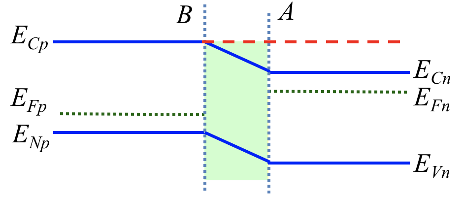
You are given the band diagram of a PN junction with doping NA and ND under forward bias of VF below. Which of the following expression correctly describe the electron concentration as described below: (a) 𝑁 𝐴 ; (b) 𝑁 𝐷 ; (c) 𝑛 𝑖 2 𝑁 𝐴 ; (d) 𝑛 𝑖 2 𝑁 𝐷 ; (e) 𝑁 𝐴 𝑒 𝑞 𝑉 𝐹 𝑘 𝑇 ; (f) 𝑁 𝐷 𝑒 𝑞 𝑉 𝐹 𝑘 𝑇 ; (g) 𝑛 𝑖 2 𝑁 𝐴 𝑒 𝑞 𝑉 𝐹 𝑘 𝑇 ; (h) 𝑛 𝑖 2 𝑁 𝐷 𝑒 𝑞 𝑉 𝐹 𝑘 𝑇 At point A above ECp (g) At point A above ECn (b) At point B above ECp (g)
View Explanation
Verified Answer
Please login to view
Step-by-Step Analysis
The question asks us to identify expressions for the electron concentration under forward bias in a PN junction, referencing specific points A and B in the band diagram. We should first separate the ideas into two regions: the p-side (p-type, doped with NA) and the n-side (n-type, doped with ND). In a forward-biased PN junction, the electron concentration on the p-side (where electrons are minority carriers) is typically proportional to the intrinsic carrier concentration n_i squared divided by the acceptor concentration, and it gains a factor e^{qV/kT} due to the applied forward voltage. Conversely, on the n-side (where electrons are majority carriers), the minority electron concentration (near the depletion edge) similarly scales with n_i^2 divided by the donor concentration, with the same e^{qV/kT} factor for forward bias. With that in mind, we evaluate each general form:
Option (a): N_A. This simply states that the electron concentration equals ......Login to view full explanationLog in for full answers
We've collected over 50,000 authentic exam questions and detailed explanations from around the globe. Log in now and get instant access to the answers!
Similar Questions
The following figure shows the electron and hole currents along the position at the n-side of a PN junction. In the figure, the depletion width is very small and not observable. Assume the diffusion coefficient and diffusion length for holes and electrons are the same (i.e. Dp=Dn and Lp=Ln). Also take kT/q=0.025V, the n-side doping concentration is ND=1x1016cm-3 and the forward voltage is 0.5V in this problem. Calculate the following (up to 3 significant digits if the answer is not a round number): 1) What is the hole current at the edge of n-side depletion region in mA? [Fill in the blank], mA 2) What is the p-side doping concentration of the PN junction? [Fill in the blank], cm-3 3) What is the new total diode current in mA if the n-side doping is increased by 10 times? [Fill in the blank], mA
The current through a PN junction under illumination can be written as, Itotal = Idiode - Iphoto where Idiode is the current given by the ideal diode equation and Iphoto is the optically generated current. When the PN junction is operated as a solar cell, which if the following statement is correct.
The carrier concentration of a PN junction is given in the figure and the minority carriers are labelled. What is the type of the given PN junction?
A high forward voltage far beyond the build-in potential is applied to a P+/N junction (assume the P+/N junction is still functioning properly and not being damaged by the high current). Which of the following action will be the most effective to further increase the current at the same voltage?
More Practical Tools for Students Powered by AI Study Helper
Making Your Study Simpler
Join us and instantly unlock extensive past papers & exclusive solutions to get a head start on your studies!